


Many materials are capable of emitting visible luminescence
when subjected to some form of excitation such as
UV light (photoluminescence), nuclear radiation such as
 rays and
 and
and  particles (scintillation), mechanical shock (triboluminescence),
heat (thermoluminescence),
chemical reactions (chemiluminescence),
and electric fields (electroluminescence).
In this section we will restrict our attention
to photoluminescence, since the interstellar
dust luminescence, as manifested by the Extended
Red Emission ubiquitously seen in interstellar
environments, is believed to be a photon-driven process
(Witt & Schild 1985;
Duley 1985;
Smith & Witt 2002;
Witt & Vijh 2004).
particles (scintillation), mechanical shock (triboluminescence),
heat (thermoluminescence),
chemical reactions (chemiluminescence),
and electric fields (electroluminescence).
In this section we will restrict our attention
to photoluminescence, since the interstellar
dust luminescence, as manifested by the Extended
Red Emission ubiquitously seen in interstellar
environments, is believed to be a photon-driven process
(Witt & Schild 1985;
Duley 1985;
Smith & Witt 2002;
Witt & Vijh 2004).
There are two pre-requisites for luminescence:
(1) the luminescent material must have a semiconductor
structure with a nonzero band gap Eg
(e.g. metals do not luminesce since they have no band gap);
(2) energy must be imparted to this material before
luminescence can take place.
The mechanism of photoluminescence in semiconductors
is schematically illustrated in Figure 8, which
plots the E-k diagrams for a direct band gap material
(left) and an indirect gap material (right),
where E and k are respectively the kinetic energy
and wave vector (or "momentum vector") of the electron
or hole (E = k2
 2 /
2m*, where
2 /
2m*, where
 h /
2
h /
2 is the Planck constant h divided by
2,
and m* is the electron or hole effective mass).
The direct and indirect gap materials
are distinguished by their relative positions
of the conduction band minimum and the valence band maximum
in the Brillouin zone (the volume of k space containing
all the values of k up to
/ a where a is
the unit lattice cell dimension).
In a direct gap material, both the conduction band
minimum and the valence band maximum occur at the zone
center where k = 0.
In an indirect gap material, however, the conduction band minimum
does not occur at k = 0, but rather at some other values of k
which is usually at the zone edge or close to it (see
Fox 2001).
is the Planck constant h divided by
2,
and m* is the electron or hole effective mass).
The direct and indirect gap materials
are distinguished by their relative positions
of the conduction band minimum and the valence band maximum
in the Brillouin zone (the volume of k space containing
all the values of k up to
/ a where a is
the unit lattice cell dimension).
In a direct gap material, both the conduction band
minimum and the valence band maximum occur at the zone
center where k = 0.
In an indirect gap material, however, the conduction band minimum
does not occur at k = 0, but rather at some other values of k
which is usually at the zone edge or close to it (see
Fox 2001).
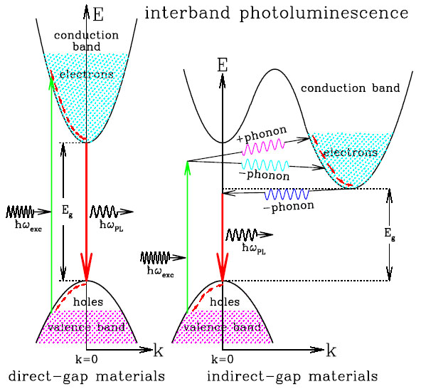 |
Figure 8. Schematic band diagrams for the
photoluminescence processes
in a direct gap material (left)
and an indirect gap material (right).
The shaded states at the bottom of the conduction band
and the empty states at the top of the valence band
respectively represent the electrons and holes
created by the absorption of photons with energy
|
Upon absorption of an UV or visible photon with an energy
 exc exceeding
the band gap Eg
(the gap in energy between the valence band and
the conduction band) of the material, an electron-hole
pair is created and the electron (hole) is excited to
states high up in the conduction (valence) band
(see Fig. 8).
exc exceeding
the band gap Eg
(the gap in energy between the valence band and
the conduction band) of the material, an electron-hole
pair is created and the electron (hole) is excited to
states high up in the conduction (valence) band
(see Fig. 8).
During a photon absorption process in semiconductors,
we must conserve both energy and momentum.
In a direct band gap material, the conduction band
minimum and the valence band maximum have the same k values
(i.e.,
 i =
f,
where
i and
f
are respectively the wave vectors
of the initial and final electron states;
this implies that the electron wave vector should not
change significantly during a photon absorption process),
conservation of momentum is guaranteed for
the photoexcitation of the electron which only
involves a UV or visible photon:
i +
phot
i =
f,
where
i and
f
are respectively the wave vectors
of the initial and final electron states;
this implies that the electron wave vector should not
change significantly during a photon absorption process),
conservation of momentum is guaranteed for
the photoexcitation of the electron which only
involves a UV or visible photon:
i +
phot
 i =
f,
since
phot,
the wave vector of the absorbed photon
(which is in the order of 2 /
i =
f,
since
phot,
the wave vector of the absorbed photon
(which is in the order of 2 /
 ~ 105
cm-1),
is negligible compared to the electron wave vector
(which is related to the size of the Brillouin zone
/ a ~ 108
cm-1, where the unit cell dimension a
is in the order of a few angstroms).
This implies that in a direct band gap material,
the electron wave vector does not change significantly
during a photon absorption process.
We therefore represent photon absorption processes
by vertical arrows in the E-k diagrams (see
Fig. 8).
~ 105
cm-1),
is negligible compared to the electron wave vector
(which is related to the size of the Brillouin zone
/ a ~ 108
cm-1, where the unit cell dimension a
is in the order of a few angstroms).
This implies that in a direct band gap material,
the electron wave vector does not change significantly
during a photon absorption process.
We therefore represent photon absorption processes
by vertical arrows in the E-k diagrams (see
Fig. 8).
In contrast, for an indirect band gap material of which
the conduction band minimum and the valence band maximum
have different k values (see Fig. 8),
conservation of momentum implies that
the photon absorption process must be assisted
by either absorbing or emitting a phonon
(a quantum of lattice vibration),
because the electron wave vector must change significantly
in jumping from the valence band in state (Ei,
i)
to a state (Ef,
f)
in the conduction band, and the absorption of a photon alone
can not provide the required momentum change since
|phot|
<<
|i
- f|.
The excited electron and hole will not remain in their initial excited states for very long; instead, they will relax very rapidly (~ 10-13 s) to the lowest energy states within their respective bands by emitting phonons. When the electron (hole) finally arrives at the bottom (top) of the conduction (valence) band, the electron-hole pair can recombine radiatively with the emission of a photon (luminescence), or nonradiatively by transferring the electron's energy to impurities or defects in the material or dangling bonds at the surface.
Just like the photon absorption process discussed above,
the electron-hole recombination in a direct band gap material
does not involve any phonons since there is no need for momentum
change for the electron. In contrast, in an indirect gap material,
the excited electron located in the conduction band needs to
undergo a change in momentum state before it can recombine with
a hole in the valence band; conservation of momentum demands
that the electron-hole recombination must be accompanied
by the emission of a phonon,
since it is not possible to make this recombination
by the emission of a photon alone.
Compared to the photon absorption process
in an indirect gap material for which conservation of
momentum can be fulfilled by either absorption or emission of
a phonon, in the electron-hole recombination process
phonon absorption becomes negligible,
whereas phonon emission becomes the dominant momentum
conservation mediator because
(1) the number of phonons available for absorption is
small and is rapidly decreasing at lower temperatures,
whereas the emission of phonons by electrons which are
already at a high-energy state is very probable;
and (2) an optical transition assisted by phonon
emission occurs at a lower photon energy Eg - h
 phon
than the gap energy, whereas phonon absorption results
in a higher photon energy of at least Eg + h
phon,
which can be more readily re-absorbed
by the semiconductor nanoparticle.
But we note that the energy of a phonon (h
phon) is
just in the order of ~ 0.01 eV, much smaller than
the energy of the electron-hole recombination luminescence photon.
Also because prior to the recombination,
the electrons and holes respectively accumulate
at the bottom of the conduction band
and the top of the valence band,
the energy separation between the electrons and the holes
approximately equals to the energy
of the band gap. Therefore, the luminescence emitted by
both types of semiconductors occurs at an energy close to
the band gap Eg.
phon
than the gap energy, whereas phonon absorption results
in a higher photon energy of at least Eg + h
phon,
which can be more readily re-absorbed
by the semiconductor nanoparticle.
But we note that the energy of a phonon (h
phon) is
just in the order of ~ 0.01 eV, much smaller than
the energy of the electron-hole recombination luminescence photon.
Also because prior to the recombination,
the electrons and holes respectively accumulate
at the bottom of the conduction band
and the top of the valence band,
the energy separation between the electrons and the holes
approximately equals to the energy
of the band gap. Therefore, the luminescence emitted by
both types of semiconductors occurs at an energy close to
the band gap Eg.
The PL efficiency is determined by the competition between radiative and nonradiative recombination. For an indirect gap material, the PL process, which requires a change in both energy and momentum for the excited electron and hence involves both a photon and a phonon, is a second-order process with a long radiative lifetime (~ 10-5 -10-3 s), and therefore a relatively small efficiency because of the competition with nonradiative combination. In contrast, in a direct gap material, the emission of a PL photon does not need the assistance of a phonon to conserve momentum. Therefore, the PL process in a direct gap material is a first-order process with a much shorter radiative lifetime (~ 10-9 -10-8 s) and a much higher PL efficiency in comparison with an indirect gap material.
However, for particles in the nanometer size domain,
we would expect substantial changes in
both the efficiency and the peak energy of
the photoluminescence due to the quantum confinement effect.
This can be understood in terms of the Heisenberg uncertainty
principle. Unlike in bulk materials the electrons and holes
are free to move within their respective bands in all three
directions, in nanoparticles the electrons and holes are
spatially confined and hence their motion is quantized in
all three dimensions.
The spatial confinement of a particle of mass m
to a region in a given direction (say, along the x axis)
of length  x
would introduce an uncertainty in its momentum
/
x
and increase its kinetic energy by an amount
EQC ~
(
px)2 / 2m ~
2 /
2m(
x)2.
A simple particle-in-a-box analysis,
using the Schrödinger's equation and the effective
mass approximation, shows that
the ground state quantum confinement energy would be
EQC ~
(3 2 /
8 m*)
( / a)2,
where m*
me*
mh* /
(me* +
mh*)
is the reduced effective mass of the electron-hole pair
(me* and
mh* are respectively the effective
mass of the electron and hole)
(Fox 2001).
For nano-sized particles, the quantum confinement
effect becomes significant since the confinement energy
EQC would be comparable to or greater than
their thermal energy
Eth ~ 3/2 kBT
at the temperature range expected for nanoparticles
in the diffuse ISM (see Figs.7, 8 of
Draine & Li 2001
and Fig. 3 of
Li & Draine 2002a).
For example, a silicon grain with
me*
0.98me
and mh*
0.52
me (me is the free electron mass)
smaller than ~ 8 nm would exhibit quantum effects at a temperature
T ~ 100 K (which is expected for
nano-sized silicon dust in the diffuse ISM;
see Fig.3 of
Li & Draine 2002a)
with
EQC
0.83(a / nm)-2 eV > Eth
0.013(T / 100
K) eV. More detailed studies show that silicon nanocrystals
exhibit an a-1.39 gap-size dependence:
Eg
E0 + 1.42(a / nm)-1.39 eV, where
E0
1.17 eV is the bulk silicon band gap
(Delerue, Allan, & Lannoo
1993).
For nanodiamonds, an a-2 gap-size dependence
was derived from the X-ray absorption
spectrum measurements
(Chang et al. 1999;
also see
Raty et al. 2003):
Eg
E0 + 0.38(a / nm)-2 eV, where
E0
5.47 eV is the bulk diamond band gap.
x
would introduce an uncertainty in its momentum
/
x
and increase its kinetic energy by an amount
EQC ~
(
px)2 / 2m ~
2 /
2m(
x)2.
A simple particle-in-a-box analysis,
using the Schrödinger's equation and the effective
mass approximation, shows that
the ground state quantum confinement energy would be
EQC ~
(3 2 /
8 m*)
( / a)2,
where m*
me*
mh* /
(me* +
mh*)
is the reduced effective mass of the electron-hole pair
(me* and
mh* are respectively the effective
mass of the electron and hole)
(Fox 2001).
For nano-sized particles, the quantum confinement
effect becomes significant since the confinement energy
EQC would be comparable to or greater than
their thermal energy
Eth ~ 3/2 kBT
at the temperature range expected for nanoparticles
in the diffuse ISM (see Figs.7, 8 of
Draine & Li 2001
and Fig. 3 of
Li & Draine 2002a).
For example, a silicon grain with
me*
0.98me
and mh*
0.52
me (me is the free electron mass)
smaller than ~ 8 nm would exhibit quantum effects at a temperature
T ~ 100 K (which is expected for
nano-sized silicon dust in the diffuse ISM;
see Fig.3 of
Li & Draine 2002a)
with
EQC
0.83(a / nm)-2 eV > Eth
0.013(T / 100
K) eV. More detailed studies show that silicon nanocrystals
exhibit an a-1.39 gap-size dependence:
Eg
E0 + 1.42(a / nm)-1.39 eV, where
E0
1.17 eV is the bulk silicon band gap
(Delerue, Allan, & Lannoo
1993).
For nanodiamonds, an a-2 gap-size dependence
was derived from the X-ray absorption
spectrum measurements
(Chang et al. 1999;
also see
Raty et al. 2003):
Eg
E0 + 0.38(a / nm)-2 eV, where
E0
5.47 eV is the bulk diamond band gap.
It is apparent, therefore, the quantum confinement effect would lead to a progressive widening of the band gap of a nano-sized semiconductor as its size is reduced, along with a broadening of the electron-hole pair state in momentum space (i.e. an increased overlap between the electron and hole wavefunctions), and a decreasing probability for the pair to find a nonradiative recombination center, provided that the surface dangling bonds are passivated which would otherwise act as traps for the carriers and quench the PL. While the former would shift the PL peak to higher energies, the latter two effects would greatly enhance the electron-hole radiative recombination probability and result in a higher PL efficiency. This is one of the main reasons why silicon nanocrystals are proposed recently by Witt and his coworkers (Witt et al. 1998, Smith & Witt 2002) and by Ledoux et al. (1998, 2001) as the ERE carrier since they are capable of luminescing very efficiently (with essentially 100% quantum efficiency) in the energy range (~ 1.4-2.4 eV) over which the ERE has been observed in astronomical sources, while bulk silicon, an indirect gap semiconductor with a band gap of ~ 1.17 eV at T = 0 K, does not luminesce.